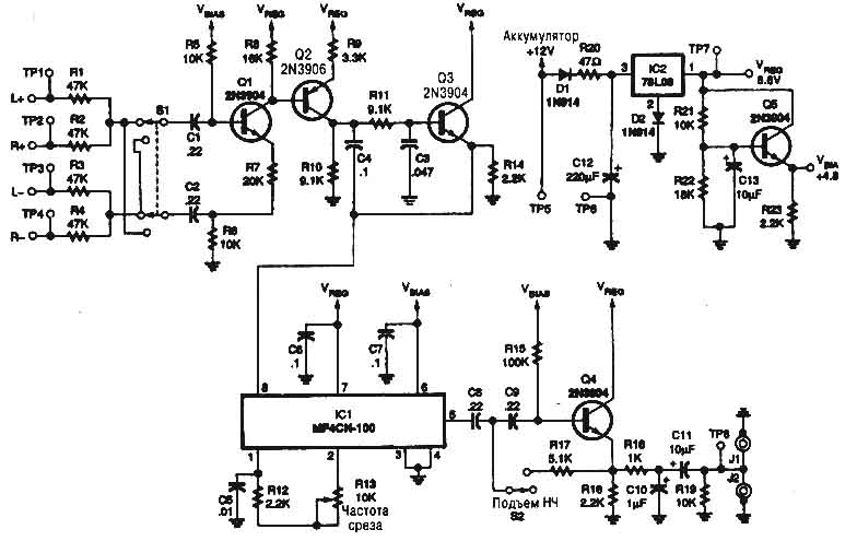
The figure shows a circuit diagram of car crossover (cr
 ossover) for the subwoofer. The input stage of the transistor Q1 is a differential summing amplifier, and the switch S1 is used to switch polarity. Switched-capacitor filter with a slope of 24 dB per octave (chip IC1) is the basis of continuously tunable filter. Potentiometer R13 controls the filter cutoff frequency on the chip IC1, adjusting its clock speed. Because the switched-capacitor filters, by definition, work with discrete signals at the input of IC1 should be restrictive filter (antialiasing). Such a low pass filter of the second order constructed by transistors Q2 and Q3 and associated elements. The output signal of IC1 via pin 5 served on a subsonic filter with the possibility of lifting the lowest frequencies. When switch S2 is closed, then on the rise of the frequency characteristic occurs. Additional filtering is provided by infrasound capacitors C1 and C2 directly to the input of the crossover. The resistor R18 and the capacitor C 10 is assembled so-called remodeling filter, eliminating the remnants of the quantization noise. The power supply circuit, gathered on the integral regulator 78L08 (chip IC2), and provides the main supply voltage of 8.6 V, and the bias voltage of 4.8 V. The diode D1 protects the circuit from negative voltage spikes and incorrect wiring. Diode D2 displaces the output reference voltage stabilizer 78L08 0.6 V for receiving an output voltage of 8.6 V, and not B. 8
Original article source cxem.net
Comments
Post a Comment