 In the development and research of electronic equipment in the laboratory one of the most important components of the measurement equipment is a universal source of test signals. Function generator, working in a range of sound frequencies, was developed based on a microcontroller. It is based on generator circuit described in [Radiohobby, 2000, № 5, p. 79]. The analysis of this scheme it was revealed a significant disadvantage. Because the counter is formed by two functional elements, the logic levels on the address pins are not installed simultaneously, which leads to the appearance of high-frequency emissions of the generator output. Developed device devoid of these deficiencies. Generated output waveform (saw, triangle, sine, square wave) programmed in flash-memory. The generator used firmware contained in [Radiohobby, 2000, № 5, p. 79]. Schematic diagram of the function generator is shown in Fig. 1.
The main technical parameters:
Range of generated frequencies, Hz
0 ... 30000
Flatness dB
<0.3
The amplitude of the output voltage, V
4
Number of steps output
128 128
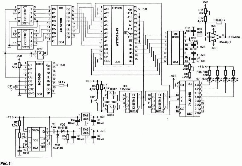
MS 4046 on a chip (DD1) assembled an oscillator, which control the frequency tuning in the range 0 ... 4 MHz. Variable resistor R1 is a multiple of the frequency control. On-chip 556IE10 (DD2) assembled address counter which outputs signals are formed ("typed address") applied to the address inputs of the PROM Winbond W27C512 (DD4). In this flash-memory chip programmed forms of output signals. With PROM outputs signals are sent to the DAC DAC0800 (DA4), from which output signal is fed to a high-speed operational amplifier K574UD1 (DA5). SB1 button is used to select the output waveform. The components of the chip 155LAZ (DD3.2, DD3.3) Assemble debounce buttons SB1. With the terminals 5 and 9, which also receives signals from the outputs of the PROM, the signal goes to the chip decoder SN74LS156N (DD7). With its removable data outputs the selected signal that displays one of the LEDs. For indicating the selected output waveform is assembled unit to the D-flip-flop circuits 155TM2 (DD6), the input of which receives impulses originating switching button. The unit is powered from the unregulated voltage source + 12, which enters the integral timer DA1 and positive voltage stabilizer DA2. Timer DA1 implemented multivibrator, the output of which removed rectangular pulses. They are rectified and is input to the negative voltage regulator DA3. The voltage from its output is used to power a generator. When setting up the device you first need to set the frequency of the selection of C1-order 4 MHz at pin 4 chips DD1, then the resistor R11 to generate sine wave mode, controlling the output of an oscilloscope, to establish the symmetry of the signal relative to the total wire. The maximum output frequency of the oscillator is determined primarily by the speed of EEPROM, which for the chip Winbond W27C512 is approximately 4 MHz, so the maximum output frequency: 4 MGts/128 stages = 30 kHz. Measured harmonic distortion of the sinusoidal signal constitute 0.0076% at 1 kHz. This generator is designed to work with a digital oscilloscope, which displays the frequency of the input signal, so additional indication output signal frequency is not provided. The devices made on microcontrollers, promising enough. For example, the proposed generator can be increased through the use of frequency oscillator with greater frequency. Also by increasing the bit of flash-memory can increase the frequency of sampling. The generator can be connected to a PC with the ability to programmatically change the shape of the output signal due to changes in firmware flash-memory. Resistor R1 - SP5-44-1 or other reusable, R9, R11 - SPZZa or other small.
Original article source cxem.net
Original article source cxem.net
Comments
Post a Comment