
The scheme is designed to protect against inrush current when the battery uncharged capacitor on-board network. Who has not tried to include uncharged faradnik network without limiting resistor - better not ... At a minimum, get burnt contacts.
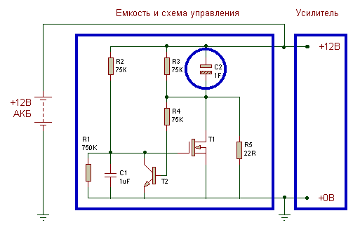
When you turn the discharged capacity in network capacity C1 is discharged, T1 (n-MOSFET switch with low channel resistance) is closed.Capacitance C2 (the same faradnik) is charged through a low-resistance R5. T2 opens almost instantly, the shunt to ground C1 and T1 gate.When the potential negative terminal C2 falls below 1V (charge to Uakb - 1B), T2 closes smoothly C1 is charged to about 9/10 Uakb opening T1. The time constant R2C1 is large enough so that the current surge T1 (pre-charge C2 +1 V to Uakb) does not exceed the rating for T1.
In the future, the negative terminal of C2 constantly shorted to ground through T1, regardless of the direction CURRENT T1 (both literally - from drain to source, and in the opposite direction). Nothing wrong with "rollover" OPEN TIR transistor not. When choosing a good enough conductive transistor entire reverse current flow through the channel, and a built-wheeling diode will not open because the voltage drop across the channel at times less than required for the opening of 0.5-0.8 V. By the way, there is a whole class of TIR devices (eg FETKY ), designed specifically to work in the opposite direction (synchronous rectifiers), they have built a diode is shunted by an additional force Schottky diode.
Calculation: for transistor IRF1010 (Rds = 0.012 ohms) voltage drop of 0.5 ohms will only be achieved with the current channel 40A (P = 20W).For four of these transistors in parallel and the same discharge current of 40A - on each transistor will dissipate 0,012 * (40/4) ^ 2 = 1.2 W, ieradiators they are not required (the more that will dissipate 1.2W only when differential current consumption but not consistently).
Dense installation (you have plenty of space for extra radiator?) - Advisable parallels small (body TO251, DIP4) transistors, generally do not provide radiators, based on the ratio of current (power) consumption of the amplifier - Rds - limit power dissipation. Since Pds max is typically 1W (800 mW for DIP4), the number of n transistors (c Rds each) for the amplifier with an output power Pout must be at least n> 1/6 * Pout * sqrt (Rds) at 12V supply (dimension in the formula I omitted). In fact, given the short duration current pulses, n can be easily reduced by half compared with a given formula.
Resistor R5 is selected from the charge compromise heat output and charging time. When these 22 ohms - charge time of about 1 minute at power dissipation 7 watts. R5 can instead include 12V bulb, say, indicator. Resistors R1, R3 - reinsurance (discharged capacity when disconnected from the network).
Connect to indicate activation of additional inverter (reducing R2). Attention! The scheme is efficient at using npn transistors T2, T3 with h21e> 200 (KT3102). Depending on the brightness of the LED, R1, select the range of 200 ohms - 1k.

But the view of the circuit in which the key shutter control signal REMOTE (And transistor). The non-connected or off REMOTE key transistor guaranteed closed. D3-D4 LEDs indicate charging C1, D5-D6 - the open state of the key.

Accurate indication of the threshold voltage is provided easiest IP TL431 (KR142EN19) in a typical mode voltage comparator (with the corresponding subgroup in the input circuit and current-limiting circuit cathode R).
Loss schemes largely depend on the installation. Ensure that the minimum resistance (and corresponding current thickness of the wires) in the power circuit (terminal + / C2 / T1 /-terminal). In amateur practice, I think, make outgoing terminals impractical - it is better to unsolder the short wires AWG8, which binds to the terminal block diagram of the amplifier.
Original article source cxem.net
Comments
Post a Comment