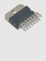
TDA7482 Audio Power Amplifier 1-channel 1 x 25W

TDA7482 general description:


The TDA7482 is an audio class-D amplifier assembled in Multiwatt15 package specially designed for high efficiency applications mainly for TV and HomeStereo sets. TDA7482 Audio Amplifier 1 x 25W

TDA7482 features:


  • 25W OUTPUT POWER:
  • RL =8Ω/4Ω; THD = 10%
  • HIGHEFFICIENCY
  • WIDE SUPPLY VOLTAGE RANGE (UP TO±25V)
  • SPLITSUPPLY
  • OVERVOLTAGEPROTECTION
  • ST-BY AND MUTEFEATURES
  • SHORTCIRCUIT PROTECTION
  • THERMALOVERLOADPROTECTION

TDA7482 circuit diagram:

TDA7482 Audio Amplifier 1 x 25W
TDA7482 Audio Amplifier 1 x 25W circuit diagram

TDA7482 sterio circuit layout:

PCB layout TDA7482 Audio Amplifier 1 x 25W
TDA7482 Audio Amplifier 1 x 25W pcb layout

Comments

Popular posts from this blog

One Chip AM/FM Radio with Audio Power Amplifier

Description: The integrated circuit TDA1083 includes, with exception  of the FM front end, a complete AM-/FM-radio-circuit  with audio power amplifier. An internal Z-diode  stabilizes the supply voltage at VS 13 V, which allows  with the aid of a resistor and a rectifier, the circuit to be  driven by a higher external supply voltage. Features: Large supply voltage range VS = 3 to 12 V High AM-Sensitivity Limiting threshold voltage Vi = 50 V Audio output power P0 = 0.7 W AFC-connection for VHF-tuner AM-FM switching without high frequency voltages Applications: AM-/FM- and audio-amplifier Circuit Diagram: Circuit diagram for One Chip AM/FM Radio with Audio Power Amplifier Datasheet for TDA1083:   Download

2 x 15 W stereo Bridge Tied Load (BTL) audio amplifier

General description: The TDA8946J is a dual-channel audio power amplifier with an output power of 2 × 15 W at an 8 Ω load and a 18 V supply. The circuit contains two Bridge Tied Load (BTL) amplifiers with an all-NPN output stage and standby/mute logic. The TDA8946J comes in a 17-pin DIL-bent-SIL (DBS) power package. The TDA8946J is printed-circuit board (PCB) compatible with all other types in the TDA894x family. One PCB footprint accommodates both the mono and the stereo products. Features: Few external components Fixed gain Standby and mute mode No on/off switching plops Low standby current High supply voltage ripple rejection Outputs short-circuit protected to ground, supply and across the load Thermally protected Printed-circuit board compatible Circuit Diagram: Circuit Diagram for 2 x 15 W stereo Bridge Tied Load (BTL) audio amplifier PCB layout: PCB layout TDA8946 Datasheet for TDA8946J:   Download

200W Hybrid Audio Amplifier Circuit

200W Hybrid Audio Amplifier Circuit - c onnecting two TDA2030 thru cheap power transistors we can create a amplifier wich can deliver a higher power. With the components value from the schematic the total amplifier gain is 32 dB. The speaker can be 2 ohm instead of 4 ohm if we use the TIP transistors. TDA 2030 is produced by SGS Ates and is a complete audio amplifier. AB class of the final amplifier cand deliver up to 14W on 4 ohm at a +-14V power supply. With a proper designed power supply this audio amplifier can output 200W. Active components: IC1, Ic2 TDA 2030 T1, T3 = BD 250, TIP 36 T2,T4 = BD 249, TIP 35 D1 … D4 = 1N4001 200W Hybrid Audio Amplifier Circuit