NCP2890 Audio Amplifier 1W

NCP2890 general description:

The NCP2890 is an audio power amplifier designed for portable communication device applications such as mobile phone applications. The NCP2890 is capable of delivering 1.0 W of continuous average power to an 8.0 BTL load from a 5.0 V power supply, and 320 mW to a 4.0 BTL load from a 2.6 V power supply. The NCP2890 provides high quality audio while requiring few external components and minimal power consumption. It features a low−power consumption shutdown mode, which is achieved by driving the SHUTDOWN pin with logic low. The NCP2890 contains circuitry to prevent from “pop and click” noise that would otherwise occur during turn−on and turn−off transitions. For maximum flexibility, the NCP2890 provides an externally controlled gain (with resistors), as well as an externally controlled turn−on time (with the bypass capacitor). Due to its excellent PSRR, it can be directly connected to the battery, saving the use of an LDO. This device is available in a 9−Pin Flip−Chip CSP (standard Tin−Lead and Lead−Free versions) and a Micro8 package. NCP2890 Audio Amplifier 1W

NCP2890 features:

  • 1.0 W to an 8.0  BTL Load from a 5.0 V Power Supply
  • Excellent PSRR: Direct Connection to the Battery
  • “Pop and Click” Noise Protection Circuit
  • Ultra Low Current Shutdown Mode
  • 2.2 V−5.5 V Operation
  • External Gain Configuration Capability
  • External Turn−on Time Configuration Capability
  • Up to 1.0 nF Capacitive Load Driving Capability
  • Thermal Overload Protection Circuitry
  • AEC−Q100 Qualified Part Available
  • Pb−Free Packages are Available
  • NCV Prefix for Automotive and Other Applications Requiring Site and Control Changes

NCP2890 aplications:

  • Portable Electronic Devices
  • PDAs
  • Wireless Phones

NCP2890 circuit diagram: 
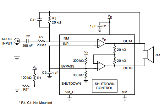
NCP2890 Audio Amplifier 1W
Circuit diagram NCP2890 Audio Amplifier 1W

NCP2890 layout pcb: 

PCB layout NCP2890 Audio Amplifier 1W
PCB layout NCP2890 Audio Amplifier 1W

Comments

Popular posts from this blog

One Chip AM/FM Radio with Audio Power Amplifier

Description: The integrated circuit TDA1083 includes, with exception  of the FM front end, a complete AM-/FM-radio-circuit  with audio power amplifier. An internal Z-diode  stabilizes the supply voltage at VS 13 V, which allows  with the aid of a resistor and a rectifier, the circuit to be  driven by a higher external supply voltage. Features: Large supply voltage range VS = 3 to 12 V High AM-Sensitivity Limiting threshold voltage Vi = 50 V Audio output power P0 = 0.7 W AFC-connection for VHF-tuner AM-FM switching without high frequency voltages Applications: AM-/FM- and audio-amplifier Circuit Diagram: Circuit diagram for One Chip AM/FM Radio with Audio Power Amplifier Datasheet for TDA1083:   Download

2 x 15 W stereo Bridge Tied Load (BTL) audio amplifier

General description: The TDA8946J is a dual-channel audio power amplifier with an output power of 2 × 15 W at an 8 Ω load and a 18 V supply. The circuit contains two Bridge Tied Load (BTL) amplifiers with an all-NPN output stage and standby/mute logic. The TDA8946J comes in a 17-pin DIL-bent-SIL (DBS) power package. The TDA8946J is printed-circuit board (PCB) compatible with all other types in the TDA894x family. One PCB footprint accommodates both the mono and the stereo products. Features: Few external components Fixed gain Standby and mute mode No on/off switching plops Low standby current High supply voltage ripple rejection Outputs short-circuit protected to ground, supply and across the load Thermally protected Printed-circuit board compatible Circuit Diagram: Circuit Diagram for 2 x 15 W stereo Bridge Tied Load (BTL) audio amplifier PCB layout: PCB layout TDA8946 Datasheet for TDA8946J:   Download

200W Hybrid Audio Amplifier Circuit

200W Hybrid Audio Amplifier Circuit - c onnecting two TDA2030 thru cheap power transistors we can create a amplifier wich can deliver a higher power. With the components value from the schematic the total amplifier gain is 32 dB. The speaker can be 2 ohm instead of 4 ohm if we use the TIP transistors. TDA 2030 is produced by SGS Ates and is a complete audio amplifier. AB class of the final amplifier cand deliver up to 14W on 4 ohm at a +-14V power supply. With a proper designed power supply this audio amplifier can output 200W. Active components: IC1, Ic2 TDA 2030 T1, T3 = BD 250, TIP 36 T2,T4 = BD 249, TIP 35 D1 … D4 = 1N4001 200W Hybrid Audio Amplifier Circuit