FEATURES:
• 5 V supply voltage
• Gain controlled wide-band Vision Intermediate Frequency (VIF) amplifier, AC-coupled
• Multistandard true synchronous demodulation with active carrier regeneration: very linear demodulation, good intermodulation figures, reduced harmonics, and excellent pulse response
• Gated phase detector for L and L-accent standard
• Fully integrated VIF Voltage Controlled Oscillator (VCO), alignment-free, frequencies switchable for all negative and positive modulated standards via I2C-bus
• Digital acquisition help, VIF frequencies of 33.4, 33.9, 38.0, 38.9, 45.75, and 58.75 MHz
• 4 MHz reference frequency input: signal from Phase-Locked Loop (PLL) tuning system or operating as crystal oscillator
• VIF Automatic Gain Control (AGC) detector for gain control, operating as peak sync detector for negative modulated signals and as a peak white detector for positive modulated signals
• VIF-AGC monitor output at pin OP2
• External VIF-AGC setting via pin OP1
• Precise fully digital Automatic Frequency Control (AFC) detector with 4-bit digital-to-analog converter, AFC bits readable via I2C-bus
• TakeOver Point (TOP) adjustable via I2C-bus or alternatively with potentiometer
• Fully integrated sound carrier trap for 4.5, 5.5, 6.0, and 6.5 MHz, controlled by FM-PLL oscillator
• Sound IF (SIF) input for single reference Quasi Split Sound (QSS) mode, PLL controlled
• SIF-AGC for gain controlled SIF amplifier, single reference QSS mixer able to operate in high performance single reference QSS mode and in intercarrier mode, switchable via I2C-bus
• AM demodulator without extra reference circuit
• Alignment-free selective FM-PLL demodulator with high linearity and low noise
• I2C-bus control for all functions
• I2C-bus transceiver with pin programmable Module Address (MAD)
• Four selectable I2C-bus addresses
• SIF and FM-AGC for radio (optional)
• Radio IF (RIF) input using the sound IF SAW input for converting to 10.7 MHz, input frequencies are 41.3 MHz for NTSC (M/N standard) applications and 33.3 MHz for other applications
• Alignment-free FM radio demodulation at 10.7 MHz
• Radio AFC
• External FM input and demodulation.
GENERAL DESCRIPTION:
The TDA9887 is an alignment-free multistandard (PAL, SECAM and NTSC) vision and sound IF signal PLL demodulator for positive and negative modulation, including sound AM and FM processing. A special function is implemented for the demodulation of FM radio signals (fRIF = 10.7 MHz).
Circuit Diagram:
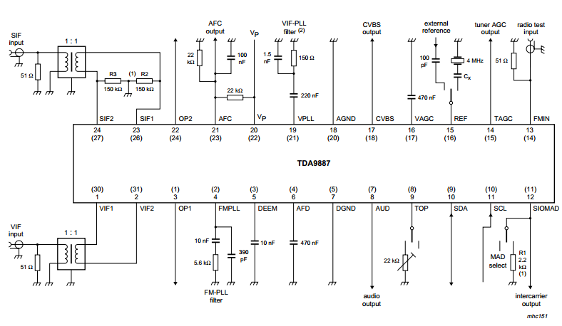 |
| I 2C-bus controlled multistandard alignment-free IF-PLL demodulator with FM radio |
Datasheet for TDA9887: Download
Comments
Post a Comment