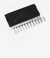
TDA8950 Audio Amplifier 2x150W

TDA8950 general description:
TDA8950 Audio Amplifier 2x150W


The TDA8950 is a high-efficiency Class D audio power amplifier. The typical output power is 2 × 150 W with a speaker load impedance of 4 Ω. The TDA8950 is available in both HSOP24 and DBS23P power packages. The amplifier operates over a wide supply voltage range from ±12.5 V to ±40 V and features low quiescent current consumption. TDA8950 Audio Amplifier 2x150W


TDA8950 features:


  • Pin compatible with TDA8920B for both HSOP24 and DBS23P packages
  • Symmetrical operating supply voltage range from ±12.5 V to ±40 V
  • Stereo full differential inputs, can be used as stereo Single-Ended (SE) or mono
  • Bridge-Tied Load (BTL) amplifier
  • High output power in typical applications:
  • SE 2 × 150 W, RL
  • 4 Ω (VP = ±37 V)
  • SE 2 × 170 W, RL
  • 4 Ω (VP = ±39 V)
  • SE 2 × 100 W, RL
  • 6 Ω (VP = ±37 V)
  • BTL 1 × 300 W, RL
  • 8 Ω (VP = ±37 V)
  • Low noise
  • Smooth pop noise-free start-up and switch off
  • Zero dead time switching
  • Fixed frequency
  • Internal or external clock
  • High efficiency
  • Low quiescent current
  • Advanced protection strategy: voltage protection and output current limiting
  • Thermal FoldBack (TFB)
  • Fixed gain of 30 dB in SE and 36 dB in BTL applications
  • Fully short-circuit proof across load
  • BD modulation in BTL configuration

Amplifier diagram, circuit for TDA8950:

TDA8950 circuit diagram
Datasheet for TDA8950: Download

Comments

Post a Comment

Popular posts from this blog

One Chip AM/FM Radio with Audio Power Amplifier

Description: The integrated circuit TDA1083 includes, with exception  of the FM front end, a complete AM-/FM-radio-circuit  with audio power amplifier. An internal Z-diode  stabilizes the supply voltage at VS 13 V, which allows  with the aid of a resistor and a rectifier, the circuit to be  driven by a higher external supply voltage. Features: Large supply voltage range VS = 3 to 12 V High AM-Sensitivity Limiting threshold voltage Vi = 50 V Audio output power P0 = 0.7 W AFC-connection for VHF-tuner AM-FM switching without high frequency voltages Applications: AM-/FM- and audio-amplifier Circuit Diagram: Circuit diagram for One Chip AM/FM Radio with Audio Power Amplifier Datasheet for TDA1083:   Download

2 x 15 W stereo Bridge Tied Load (BTL) audio amplifier

General description: The TDA8946J is a dual-channel audio power amplifier with an output power of 2 × 15 W at an 8 Ω load and a 18 V supply. The circuit contains two Bridge Tied Load (BTL) amplifiers with an all-NPN output stage and standby/mute logic. The TDA8946J comes in a 17-pin DIL-bent-SIL (DBS) power package. The TDA8946J is printed-circuit board (PCB) compatible with all other types in the TDA894x family. One PCB footprint accommodates both the mono and the stereo products. Features: Few external components Fixed gain Standby and mute mode No on/off switching plops Low standby current High supply voltage ripple rejection Outputs short-circuit protected to ground, supply and across the load Thermally protected Printed-circuit board compatible Circuit Diagram: Circuit Diagram for 2 x 15 W stereo Bridge Tied Load (BTL) audio amplifier PCB layout: PCB layout TDA8946 Datasheet for TDA8946J:   Download

200W Hybrid Audio Amplifier Circuit

200W Hybrid Audio Amplifier Circuit - c onnecting two TDA2030 thru cheap power transistors we can create a amplifier wich can deliver a higher power. With the components value from the schematic the total amplifier gain is 32 dB. The speaker can be 2 ohm instead of 4 ohm if we use the TIP transistors. TDA 2030 is produced by SGS Ates and is a complete audio amplifier. AB class of the final amplifier cand deliver up to 14W on 4 ohm at a +-14V power supply. With a proper designed power supply this audio amplifier can output 200W. Active components: IC1, Ic2 TDA 2030 T1, T3 = BD 250, TIP 36 T2,T4 = BD 249, TIP 35 D1 … D4 = 1N4001 200W Hybrid Audio Amplifier Circuit