TDA1566 Audio Amplifier 2x46W / 1x92W

TDA1566 general description:


The TDA1566 is a car audio power amplifier with a complementary output stage realized in BCDMOS. The TDA1566 has two Bridge Tied Load (BTL) output stages and comes in a HSOP24 or DBS27P package. The TDA1566 can be controlled with or without I2C-bus. With I2C-bus control gain settings per channel and diagnostic trigger levels can be selected. Failure conditions as well as load identification can be read with I2C-bus. The load identification detects whether the outputs of a BTL channel are connected with a DC or AC load and discriminates between a speaker load, a line driver load and an open (unconnected) load. The TDA1566 can be configured in a single BTL mode and drive a 1 Ω load. For the single BTL mode it is necessary to connect on the Printed-Circuit Board (PCB) the outputs of both BTL channels in parallel.  TDA1566 Audio Amplifier 2x46W / 1x92W

TDA1566 features:


  • Operates in I2C-bus mode and non-I2C-bus mode
  • TH version: four I2C-bus addresses controlled by two pins; J version: two I2C-busaddresses controlled by one pin
  • Two 4 Ω or 2 Ω capable BTL channels or one 1 Ω capable BTL channel
  • Low offset
  • Pop free off/standby/mute/operating mode transitions
  • Speaker fault detection
  • Selectable gain (26 dB and 16 dB)
  • In I2C-bus mode:
  • DC load detection: open, short and speaker or line driver present
  • AC load (tweeter) detection
  • Programmable trigger levels for DC and AC load detection
  • Per channel programmable gain (26 dB and 16 dB, selectable per channel)
  • Selectable diagnostic levels for clip detection and thermal pre-warning
  • Selectable information on the DIAG pin for clip information of each channelseparately and independent enabling of thermal-, offset- or load fault
  • Independent short-circuit protection per channel
  • Loss of ground and open VP safe
  • All outputs short-circuit proof to VP, GND and across the load
  • All pins short-circuit proof to ground
  • Temperature controlled gain reduction at high junction temperatures
  • Fault condition diagnosis per channel: short to ground, short to supply, shorted leadand speaker fault (wrongly connected)
  • Low battery voltage detection
  • TH version: pin compatible with the TDA8566TH1

TDA1566 circuit:
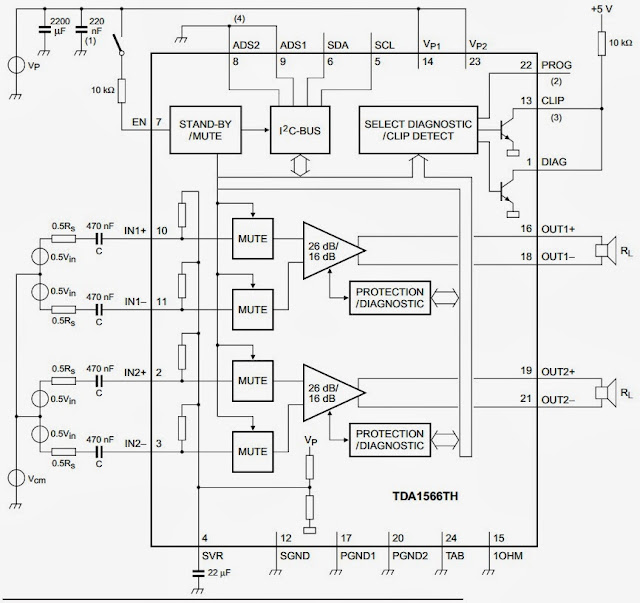
TDA1566 Audio Amplifier 2x46W


TDA1566 Audio Amplifier 2x46W

TDA1566 layout:

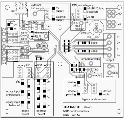
TDA1566 Audio Amplifier 2x46W layout
TDA1566 Audio Amplifier 2x46W pcb


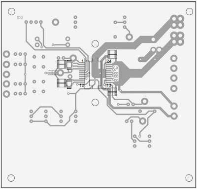
TDA1566 Audio Amplifier 2x46WTDA1566 Audio Amplifier 2x46W pcb


TDA1566 Audio Amplifier 2x46W pcb


Comments

Popular posts from this blog

One Chip AM/FM Radio with Audio Power Amplifier

Description: The integrated circuit TDA1083 includes, with exception  of the FM front end, a complete AM-/FM-radio-circuit  with audio power amplifier. An internal Z-diode  stabilizes the supply voltage at VS 13 V, which allows  with the aid of a resistor and a rectifier, the circuit to be  driven by a higher external supply voltage. Features: Large supply voltage range VS = 3 to 12 V High AM-Sensitivity Limiting threshold voltage Vi = 50 V Audio output power P0 = 0.7 W AFC-connection for VHF-tuner AM-FM switching without high frequency voltages Applications: AM-/FM- and audio-amplifier Circuit Diagram: Circuit diagram for One Chip AM/FM Radio with Audio Power Amplifier Datasheet for TDA1083:   Download

2 x 15 W stereo Bridge Tied Load (BTL) audio amplifier

General description: The TDA8946J is a dual-channel audio power amplifier with an output power of 2 × 15 W at an 8 Ω load and a 18 V supply. The circuit contains two Bridge Tied Load (BTL) amplifiers with an all-NPN output stage and standby/mute logic. The TDA8946J comes in a 17-pin DIL-bent-SIL (DBS) power package. The TDA8946J is printed-circuit board (PCB) compatible with all other types in the TDA894x family. One PCB footprint accommodates both the mono and the stereo products. Features: Few external components Fixed gain Standby and mute mode No on/off switching plops Low standby current High supply voltage ripple rejection Outputs short-circuit protected to ground, supply and across the load Thermally protected Printed-circuit board compatible Circuit Diagram: Circuit Diagram for 2 x 15 W stereo Bridge Tied Load (BTL) audio amplifier PCB layout: PCB layout TDA8946 Datasheet for TDA8946J:   Download

200W Hybrid Audio Amplifier Circuit

200W Hybrid Audio Amplifier Circuit - c onnecting two TDA2030 thru cheap power transistors we can create a amplifier wich can deliver a higher power. With the components value from the schematic the total amplifier gain is 32 dB. The speaker can be 2 ohm instead of 4 ohm if we use the TIP transistors. TDA 2030 is produced by SGS Ates and is a complete audio amplifier. AB class of the final amplifier cand deliver up to 14W on 4 ohm at a +-14V power supply. With a proper designed power supply this audio amplifier can output 200W. Active components: IC1, Ic2 TDA 2030 T1, T3 = BD 250, TIP 36 T2,T4 = BD 249, TIP 35 D1 … D4 = 1N4001 200W Hybrid Audio Amplifier Circuit