TDA1015 Audio Amplifier 1x4W

TDA1015 general description:


The TDA1015 is a monolithic integrated audio amplifier circuit in a 9-lead single in-line (SIL) plastic package. The device is especially designed for portable radio and recorder applications and delivers up to 4 W in a 4Ω load impedance. The very low applicable supply voltage of 3,6 V permits 6 V spplications.

TDA1015 features:


  • single in-line (SIL) construction for easy mounting
  • separated preamplifier and power amplifier
  • high output power
  • thermal protection
  • high input impedance
  • low current drain
  • limited noise behaviour at radio frequencies

TDA1015 reference data:


  • Supply voltage range VP 3,6 to 18 V
  • Peak output current IOM max. 2,5 A
  • Output power at dtot= 10%
  • VP = 12 V; RL = 4 Ω Po typ. 4,2 W
  • VP = 9 V; RL = 4 Ω Po typ. 2,3 W
  • VP = 6 V; RL = 4 Ω Po typ. 1,0 W
  • Total harmonic distortion at Po = 1 W; RL = 4 Ω dtot typ. 0,3 %
  • Input impedance preamplifier (pin 8) |Zi | > 100 kΩ power amplifier (pin 6) |Zi| typ. 20 kΩ
  • Total quiescent current Itot typ. 14 mA
  • Operating ambient temperature Tamb −25 to + 150 °C
  • Storage temperature Tstg −55 to + 150 °C

TDA1015 circuit diagram:
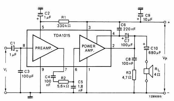
Circuit diagram TDA1015 Audio Amplifier 1x4W

Comments

Popular posts from this blog

One Chip AM/FM Radio with Audio Power Amplifier

Description: The integrated circuit TDA1083 includes, with exception  of the FM front end, a complete AM-/FM-radio-circuit  with audio power amplifier. An internal Z-diode  stabilizes the supply voltage at VS 13 V, which allows  with the aid of a resistor and a rectifier, the circuit to be  driven by a higher external supply voltage. Features: Large supply voltage range VS = 3 to 12 V High AM-Sensitivity Limiting threshold voltage Vi = 50 V Audio output power P0 = 0.7 W AFC-connection for VHF-tuner AM-FM switching without high frequency voltages Applications: AM-/FM- and audio-amplifier Circuit Diagram: Circuit diagram for One Chip AM/FM Radio with Audio Power Amplifier Datasheet for TDA1083:   Download

2 x 15 W stereo Bridge Tied Load (BTL) audio amplifier

General description: The TDA8946J is a dual-channel audio power amplifier with an output power of 2 × 15 W at an 8 Ω load and a 18 V supply. The circuit contains two Bridge Tied Load (BTL) amplifiers with an all-NPN output stage and standby/mute logic. The TDA8946J comes in a 17-pin DIL-bent-SIL (DBS) power package. The TDA8946J is printed-circuit board (PCB) compatible with all other types in the TDA894x family. One PCB footprint accommodates both the mono and the stereo products. Features: Few external components Fixed gain Standby and mute mode No on/off switching plops Low standby current High supply voltage ripple rejection Outputs short-circuit protected to ground, supply and across the load Thermally protected Printed-circuit board compatible Circuit Diagram: Circuit Diagram for 2 x 15 W stereo Bridge Tied Load (BTL) audio amplifier PCB layout: PCB layout TDA8946 Datasheet for TDA8946J:   Download

200W Hybrid Audio Amplifier Circuit

200W Hybrid Audio Amplifier Circuit - c onnecting two TDA2030 thru cheap power transistors we can create a amplifier wich can deliver a higher power. With the components value from the schematic the total amplifier gain is 32 dB. The speaker can be 2 ohm instead of 4 ohm if we use the TIP transistors. TDA 2030 is produced by SGS Ates and is a complete audio amplifier. AB class of the final amplifier cand deliver up to 14W on 4 ohm at a +-14V power supply. With a proper designed power supply this audio amplifier can output 200W. Active components: IC1, Ic2 TDA 2030 T1, T3 = BD 250, TIP 36 T2,T4 = BD 249, TIP 35 D1 … D4 = 1N4001 200W Hybrid Audio Amplifier Circuit