
LM4702 Amplifier Circuit Diagram

LM4702 general description:

     The LM4702 is a high fidelity audio power amplifier driver designed for demanding consumer and pro-audio applications. Amplifier output power may be scaled by changing the supply voltage and number of output devices. The LM4702 is capable of delivering in excess of 300 watts per channel single ended into an 8 ohm load in the presence of 10% high line headroom and 20% supply regulation. The LM4702 includes thermal shut down circuitry that activates when the die temperature exceeds 150°C. The LM4702's mute function, when activated, mutes the input drive signal and forces the amplifier output to a quiescent state. The LM4702 is available in 3 grades that span a wide range of applications and performance levels. The LM4702C is targeted at high volume applications. The LM4702B includes a higher voltage rating along – LM4702A (1) (in development): with the tighter specifications. The LM4702A(1) (in ±20V to ±100V development) is the premium part with the highest voltage rating, fully specified with limits over voltage – LM4702B: ±20V to ±100V and temperature, and is offered in a military 883 – LM4702C: ±20V to ±75V compliant TO-3 package.

LM4702 features:

  • Very High Voltage Operation
  • Scalable Output Power
  • Minimum External Components
  • External Compensation
  • Thermal Shutdown and Mute

LM4702 applications:

  • AV Receivers
  • Audiophile Power Amps
  • Pro Audio
  • High Voltage Industrial Applications

LM4702 circuit diagram:

Typical Audio Amplifier Application Circuit

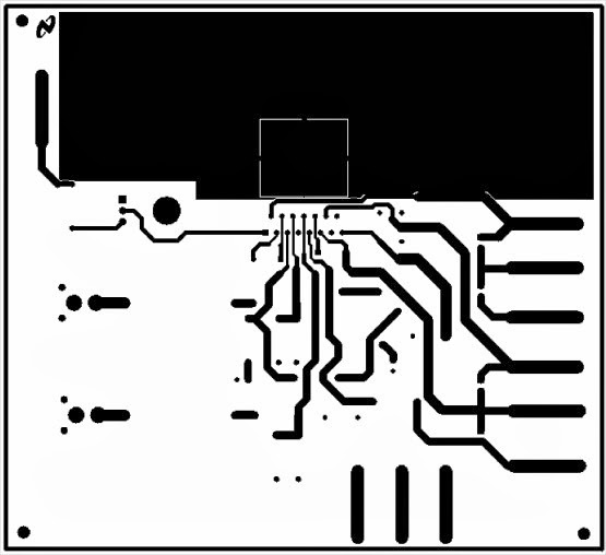
LM4702 layout and pcb:

LM4702 layout


LM4702 bottom pcb
LM4702 top pcb


Блок питания усилителя

LM4702 Audio Power Amplifier Datasheet - Download


Searches related to LM4702 Amplifier Circuit Diagram

lm4702 bridge amplifier   
lm4702 pcb
lm4702 price
lm4702 equivalent
lm4702 replacement
lm4702 datasheet
1000 watts power amplifier schematic diagram
lm4702 mosfet amplifier

Circuit Archives - Amplifier Circuit Design

Audio Power Amplifier Driver
Audio Power Amplifier Series Stereo High Fidelity 200 Volt ...
MOSFET Bridge Power Amplifier - Forum for Electronics

Comments

Popular posts from this blog

One Chip AM/FM Radio with Audio Power Amplifier

Description: The integrated circuit TDA1083 includes, with exception  of the FM front end, a complete AM-/FM-radio-circuit  with audio power amplifier. An internal Z-diode  stabilizes the supply voltage at VS 13 V, which allows  with the aid of a resistor and a rectifier, the circuit to be  driven by a higher external supply voltage. Features: Large supply voltage range VS = 3 to 12 V High AM-Sensitivity Limiting threshold voltage Vi = 50 V Audio output power P0 = 0.7 W AFC-connection for VHF-tuner AM-FM switching without high frequency voltages Applications: AM-/FM- and audio-amplifier Circuit Diagram: Circuit diagram for One Chip AM/FM Radio with Audio Power Amplifier Datasheet for TDA1083:   Download

2 x 15 W stereo Bridge Tied Load (BTL) audio amplifier

General description: The TDA8946J is a dual-channel audio power amplifier with an output power of 2 × 15 W at an 8 Ω load and a 18 V supply. The circuit contains two Bridge Tied Load (BTL) amplifiers with an all-NPN output stage and standby/mute logic. The TDA8946J comes in a 17-pin DIL-bent-SIL (DBS) power package. The TDA8946J is printed-circuit board (PCB) compatible with all other types in the TDA894x family. One PCB footprint accommodates both the mono and the stereo products. Features: Few external components Fixed gain Standby and mute mode No on/off switching plops Low standby current High supply voltage ripple rejection Outputs short-circuit protected to ground, supply and across the load Thermally protected Printed-circuit board compatible Circuit Diagram: Circuit Diagram for 2 x 15 W stereo Bridge Tied Load (BTL) audio amplifier PCB layout: PCB layout TDA8946 Datasheet for TDA8946J:   Download

200W Hybrid Audio Amplifier Circuit

200W Hybrid Audio Amplifier Circuit - c onnecting two TDA2030 thru cheap power transistors we can create a amplifier wich can deliver a higher power. With the components value from the schematic the total amplifier gain is 32 dB. The speaker can be 2 ohm instead of 4 ohm if we use the TIP transistors. TDA 2030 is produced by SGS Ates and is a complete audio amplifier. AB class of the final amplifier cand deliver up to 14W on 4 ohm at a +-14V power supply. With a proper designed power supply this audio amplifier can output 200W. Active components: IC1, Ic2 TDA 2030 T1, T3 = BD 250, TIP 36 T2,T4 = BD 249, TIP 35 D1 … D4 = 1N4001 200W Hybrid Audio Amplifier Circuit